


Назначение диода — проводить электрический ток только в одном направлении. Когда-то давно применялись ламповые диоды. Но сейчас используются в основном полупроводниковые диоды. В отличие от ламповых они значительно меньше по размеру, не требуют цепей накала и их очень просто соединять различным образом.
Условное обозначение
диода на схеме
На рисунке показано условное обозначение диода на схеме. Буквами А и К соответственно обозначены анод диода и катод диода. Анод диода — это вывод, который подключается к положительному выводу источника питания, непосредственно или через элементы схемы. Катод диода — это вывод из которого выходит ток положительного потенциала и далее через элементы схемы попадает на отрицательный электрод источника тока. Т.е. ток через диод
Как проверить диод мультиметром
Выводы диода
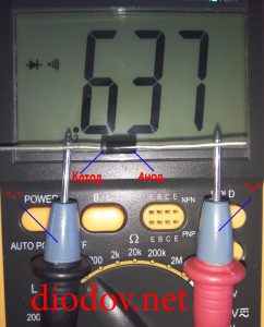
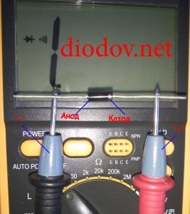
Как проверить диод мультиметром или тестером — такой вопрос встаёт тогда, когда есть подозрение, что диод неисправен. Но, ответ на этот вопрос даёт ещё один ответ, где у диода анод, а где катод. Т.е. если мы изначально не знаем цоколёвку диода, то просто ставим мультиметр или тестер на прозвонку диодов (или на измерение сопротивления) и по очереди прозваниваем диод в обоих направлениях. Если диод исправен, наш прибор будет показывать прохождение тока только в одном из вариантов. Если диод пропускает ток в обоих вариантах — диод пробит. Если он не пропускает ни в каком варианте, диод перегорел и также неисправен. В случае исправного диода, когда он проводит ток, смотрим на клеммы прибора, тот вывод диода, что подключен к положительному выводу тестера, является анодом диода, а тот, что к отрицательному — катодом диода. Проверка диодов очень похожа на проверку транзисторов.
Куда течет ток или где же этот чертов катод? / Хабр
Есть вещи, которые хочется, что называется «развидеть» — термин вполне устоявшийся и понятный.— Евгений Гришковец, рассказывает про железнодорожников. (с) Спектакль «Одновременно»
А есть вещи которые, ну никак не получается запомнить. Это возникает от того, что новое понятие не может однозначно зацепиться за уже известные факты в сознании, никак не получается построить новую связь в семантической сети фактов.
Все знают, что у диода есть катод и анод. Все знают, как диод обозначается на электрической схеме. Но далеко не все могут правильно сказать, где же на схеме что.
Под спойлером картинка, посмотрев на которую, вы навсегда запомните, где у диода анод, а где катод. Должен предупредить, развидеть это не получится, так что тот, кто не уверен в себе, пусть не открывает.
Да, вот так все просто. Буква К — это катод, буква А — это анод. Извините, теперь и вы это никогда не забудете.
Продолжим, и разберемся куда течет ток. Если приглядеться, обозначение диода представляет собой стрелку. Вот, не поверите — ток течет именно туда, куда показывает стрелка! Что логично, не правда ли? Дальше больше — ток течет «Аткуда» (от Анода) и «Куда» (к Катоду). В обозначениях транзисторов тоже есть стрелки, и они так же обозначают направление тока.
Ток — направленное движение заряженных частиц — это мы все знаем из школьной физики. Каких частиц? Да, любых заряженных! Это могут быть и электроны несущие отрицательный заряд и обделенные электронами частицы — атомы или молекулы, в растворах и плазме — ионы, в полупроводниках — «свободные электроны» или вообще «дырки», что бы это не значило. Так вот, во всем этом зоопарке проще всего разобраться так: ток течет от плюса к минусу, и все. Запомнить это очень просто: «плюс» — интуитивно — это там где чего-то «больше», больше в данном случае зарядов (еще раз — не важно каких!) и текут они в сторону «минуса», где их мало и ждут. Все остальные подробности, непринципиальны.
Ну, и последнее — батарейка. Обозначение тоже всем известно, две палочки подлинней потоньше и покороче потолще. Так вот покороче и потолще символизирует собой минус — эдакий «жирный минус» — как в школе, помните: «ставлю тебе четыре
Теперь, вы без труда ответите на вопрос, загорится ли лампочка в этой схеме:
Всех с 1 апреля! Улыбайтесь, господа. Улыбайтесь!
Что такое анод и катод — простое объяснение

Простое объяснение понятий анод и катод. Как их легко определить и запомнить.
Среди терминов в электрике встречаются такие понятия как анод и катод. Это касается источников питания, гальваники, химии и физики. Термин встречается также в вакуумной и полупроводниковой электронике. Им обозначают выводы или контакты устройств и каким электрическим знаком они обладают. В этой статье мы расскажем, что это такое анод и катод, а также как определить где они находятся в электролизере, диоде и у батарейки, что из них плюс, а что минус. Содержание:
Электрохимия и гальваника
В электрохимии есть два основных раздела:
- Гальванические элементы – производство электричества за счет химической реакции. К таким элементам относятся батарейки и аккумуляторы. Их часто называют химическими источниками тока.
- Электролиз – воздействие на химическую реакцию электроэнергией, простыми словами – с помощью источника питания запускается какая-то реакция.
Рассмотрим окислительно-восстановительную реакцию в гальваническом элементе, тогда какие процессы протекают на его электродах?
- Анод – электрод на котором наблюдается окислительная реакция, то есть он отдаёт электроны. Электрод, на котором происходит окислительная реакция – называется восстановителем.
- Катод – электрод на котором протекает восстановительная реакция, то есть он принимает электроны. Электрод, на котором происходит восстановительная реакция – называется окислителем.
Отсюда возникает вопрос – где плюс, а где минус у батарейки? Исходя из определения, у гальванического элемента анод отдаёт электроны.
Важно! В ГОСТ 15596-82 дано официальное определение названий выводов химических источников тока, если кратко, то плюс на катоде, а минус на аноде.
В данном случае рассматривается протекание электрического тока по проводнику внешней цепи от окислителя (катода) к восстановителю (аноду). Так как электроны в цепи текут от минуса к плюсу, а электрический ток наоборот, тогда катод – это плюс, а анод – это минус.

Внимание: ток всегда втекает в анод!
Или то же самое на схеме:

Процесс электролиза или зарядки аккумулятора
Эти процессы похожи и обратны гальваническому элементу, поскольку здесь не энергия поступает за счет химической реакции, а наоборот – химическая реакция происходит за счет внешнего источника электричества.
В этом случае плюс источника питания всё также называется катодом, а минус анодом. Зато контакты заряжаемого гальванического элемента или электроды электролизера уже будут носить противоположные названия, давайте разберемся почему!
Важно! При разряде гальванического элемента анод – минус, катод – плюс, при зарядке наоборот.
Так как ток от плюсового вывода источника питания поступает на плюсовой вывод аккумулятора – последний уже не может быть катодом. Ссылаясь на вышесказанное можно сделать вывод, что в этом случае электроды аккумулятора при зарядке условно меняются местами.
Тогда через электрод заряжаемого гальванического элемента, в который втекает электрический ток, называют анодом. Получается, что при зарядке у аккумулятора плюс становится анодом, а минус катодом.

Гальванотехника
Процессы осаждения металлов в результате химической реакции под воздействием электрического тока (при электролизе) называют гальванотехникой. Таким образом мир получил посеребренные, золоченные, хромированные или покрытые другими металлами украшения и детали. Этот процесс используют как в декоративных, так и в прикладных целях – для улучшения стойкости к коррозии различных узлов и агрегатов механизмов.

Принцип действия установок для нанесения гальванического покрытия лежит в использовании растворов солей элементов, которыми будут покрывать деталь, в качестве электролита.
В гальванике анод также является электродом, к которому подключаются плюсовой вывод источника питания, соответственно катод в этом случае – это минус. При этом металл осаждается (восстанавливается) на минусовом электроде (реакция восстановления). То есть если вы хотите сделать позолоченное кольцо своими руками – подключите к нему минусовой вывод блока питания и поместите в ёмкость с соответствующим раствором.
В электронике
Электроды или ножки полупроводниковых и вакуумных электронных приборов тоже часто называют анодом и катодом. Рассмотрим условное графическое обозначение полупроводникового диода на схеме:

Как мы видим, анод у диода подключается к плюсу батареи. Он так называется по той же причине – в этот вывод у диода в любом случае втекает ток. На реальном элементе на катоде есть маркировка в виде полосы или точки.

У светодиода аналогично. На 5 мм светодиодах внутренности видны через колбу. Та половина, что больше — это катод.

Также обстоит ситуация и с тиристором, назначение выводов и «однополярное» применение этих трёхногих компонентов делают его управляемым диодом:

У вакуумного диода анод тоже подключается к плюсу, а катод к минусу, что изображено на схеме ниже. Хотя при приложении обратного напряжения – названия этих элементов не изменятся, несмотря на протекание электрического тока в обратном направлении, пусть и незначительного.

С пассивными элементами, такими как конденсаторы и резисторы дело обстоит иначе. У резистора не выделяют отдельно катод и анод, ток в нём может протекать в любом направлении. Вы можете дать любые названия его выводам, в зависимости от ситуации и рассматриваемой схемы. У обычных неполярных конденсаторов также. Реже такое разделение по названиям контактов наблюдается в электролитических конденсаторах.

Заключение

Во всех перечисленных случаях ток вытекает из катода, а втекает в анод.
Пусть вас не собьёт с толку путаница: «почему у аккумулятора катод положительный, а когда его заряжают – он становится отрицательным?». Помните у всех элементов электроники, а также электролизеров и в гальванике – в общем у всех потребителей энергии анодом называют вывод, подключаемый к плюсу. На этом отличия заканчиваются, теперь вам проще разобраться что плюс, что минус между выводами элементов и устройств.
Напоследок рекомендуем просмотреть полезное видео по теме статьи:
Теперь вы знаете, что такое анод и катод, а также как запомнить их достаточно быстро. Надеемся, предоставленная информация была для вас полезной и интересной!
Материалы по теме:
- Чем отличается переменный ток от постоянного
- Фазное и линейное напряжение в сети
- Как зарядить батарейку в домашних условиях
 0)Не нравится
Стабилитрон относится к одному из применяемых радиоэлектронных элементов. Каждый более-менее качественный блок питания содержит узел стабилизации напряжения, которое может изменяться при изменении сопротивления нагрузки либо при отклонении входного напряжения от номинального значения.

Стабилизация напряжения выполняется главным образом с целью обеспечения нормального режима работы остальных радиоэлементов устройства, например микросхем, транзисторов, микроконтроллеров и т.п.
Стабилитроны широко используются в маломощных блоках питания либо в отдельных его узлах, мощность которых редко превышает десятки ватт.
Главное преимущество стабилитронов – их малая стоимость и габариты, поэтому они до сих пор не могут вытисниться интегральными стабилизаторами напряжения типа LM7805 или 78L05 и т.п.
Стабилитрон очень похож на диод, поскольку его полупроводниковый кристалл помещен в аналогичный корпус.
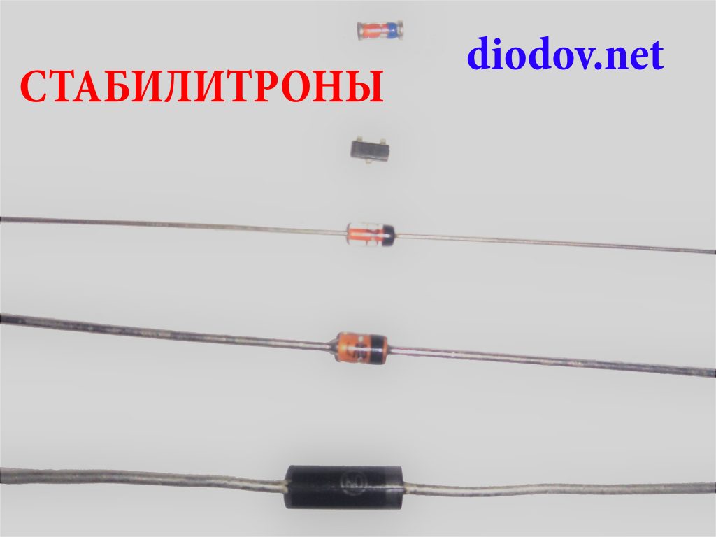
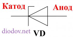
Условное графическое обозначение стабилитрона на чертежах электрических схем также похоже на обозначение диода, только со стороны катода добавлена короткая горизонтальная черточка, направленная в сторону анода.
Принцип работы стабилитрона
Рассмотрим принцип работы стабилитрона на примере схемы его включения и вольт-амперной характеристике. Для выполнения своей основной функции стабилитрон VD соединяется последовательно с резистором Rб и вместе они подключаются к источнику входного нестабилизированного напряжения Uвх. Уже стабилизированное выходное напряжение Uвых снимается только с выводов
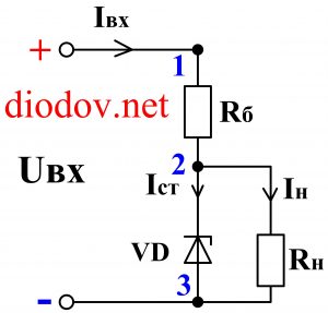
Величина напряжения Uвх, подаваемого на стабилитрон с резисторов должна быть выше на минимум на пару вольт выходного напряжения Uвых, в противном случае полупроводниковый прибор VD не откроется и не сможет выполнять свою основную функцию.
Допустим, в какой-то произвольный момент времени на выходах 1 и 3 значение Uвх начало возрастать. В схеме начнут протекать следующие процессы. С ростом напряжения согласно закону Ома начнет возрастать ток, назовем его входным током Iвх. С увеличением ток возрастет падение напряжения на резисторе Rб, а на VD она останется неизменным (это будет пояснено далее на характеристике), поэтому и Uвых останется на прежнем уровне. Следовательно, прирост входного напряжения упадет или погасится на резисторе Rб. Поэтому Rб называют гасящим или балластным.
Теперь, допустим, изменилась нагрузка, например, снизилось сопротивление Rн, соответственно возрастет и ток Iн. В этом случае снизится ток, протекающий стабилитрон Iст, а Iвх останется практически без изменений.
Вольт-амперная характеристика стабилитрона
Вольт-амперная характеристика (ВАХ) стабилитрона аналогично ВАХ диода и имеет две ветви: прямую и обратную. Прямая ветвь является рабочей для диода, а обратная ветвь характеризует работу стабилитрона, поэтому он включается в электрическую цепь в обратном направлении (катодом к плюсу, а анодом к минусу) по сравнению с диодом. Поэтому стабилитрон называю опорным диодом, а источник питания с данным полупроводниковым элементом называют опорным источником напряжения. Такой терминологий будем пользоваться и мы.
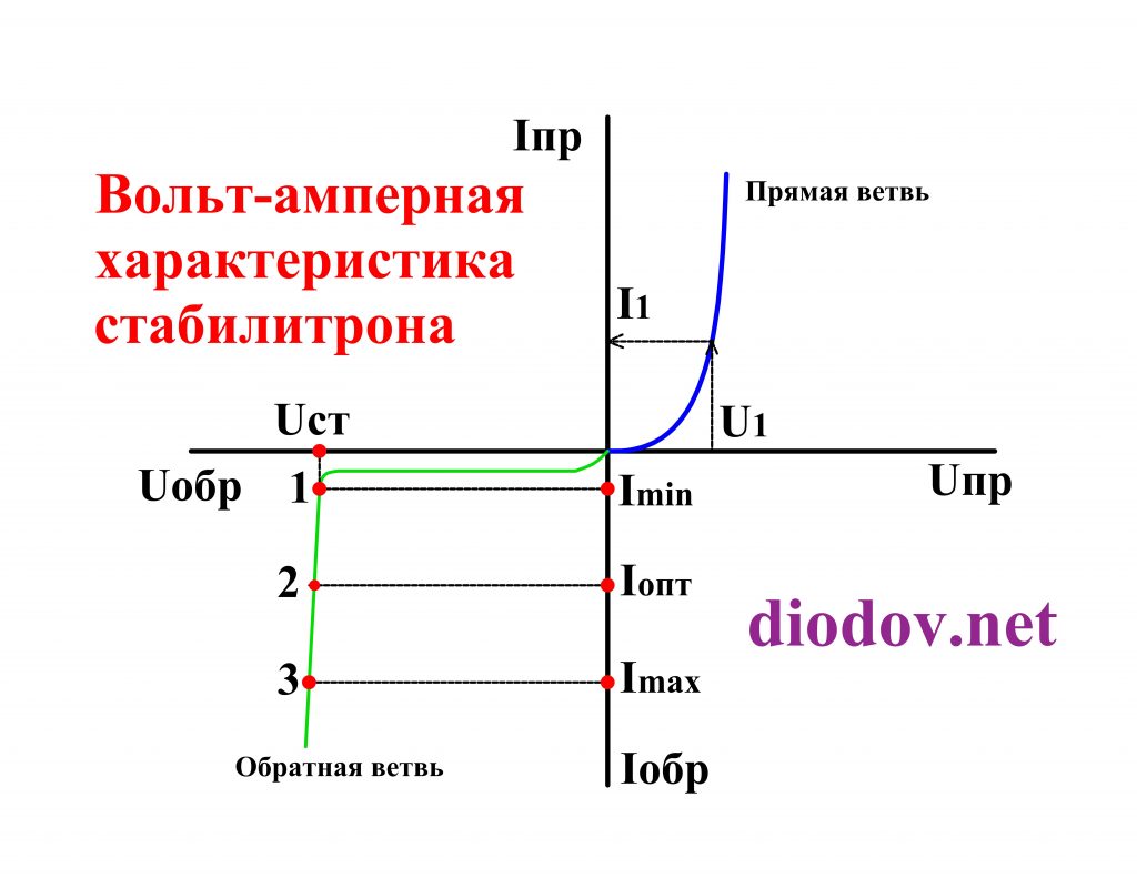
На обратной ветви вольт-амперной характеристик опорного диода выделим две характерные точки 1 и 3. Точка 1 отвечает минимальному значению тока стабилизации, который находится в пределах единиц миллиампер. Если ток, протекающий через стабилитрон, будет ниже точки 1, то он не сможет выполнять свои функции (не откроется). В случае превышения тока выше точки 3 опорный диод перегреется и выйдет из строя. Поэтому оптимальной точкой в большинстве случае будет точка посредине обратной ветви ВАХ, то есть точка 2. Тогда при изменении тока в широких пределах (смотрите ось Y) точка 2 будет изменять свое положение, перемещаясь вверх или вниз по обратной ветви, а напряжение будет изменяться незначительно (смотрите ось X).
Встречное, параллельное, последовательное соединение стабилитронов
Для повышения напряжения стабилизации можно последовательно соединять два и более стабилитрона. Например на нагрузке нужно получить 17 В, тогда, в случае отсутствия нужного номинала, применяют опорные диоды на 5,1 В и на 12 В.
Параллельное соединение применяется с целью повышения тока и мощности.
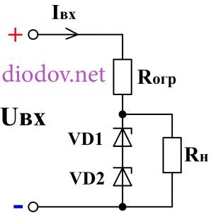
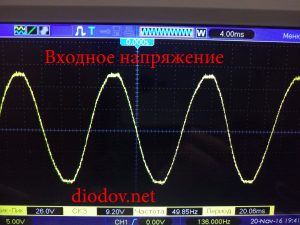
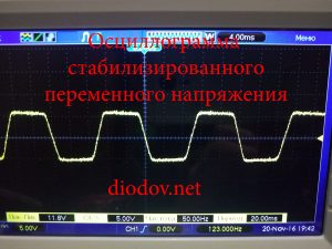
Также стабилитроны находят применение для стабилизации переменного напряжения. В этом случае они соединяются последовательно и встречно.
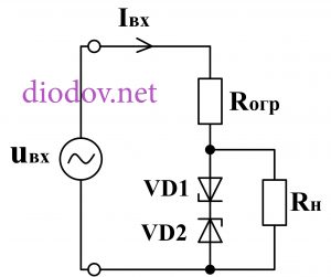
В один полупериод переменного напряжения работает один стабилитрон, а второй работает как обычный диод. Во второй полупериод полупроводниковые элементы выполняют противоположные функции. Однако в таком случае форма выходного напряжения будет отличается от входного и выглядит как трапеция. За счет того, что опорный диод будет отсекать напряжение, превышающее уровень стабилизации, верхушки синусоиды будут срезаться.
Маркировка стабилитронов
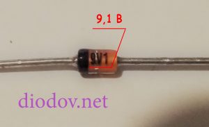
Маркировка наносится на корпус стабилитрона в виде цифр и букв (или буквы). Различают принципиально два разных типа маркировки. Стабилитрон в стеклянном корпусе имеет привычную для нас маркировку, непосредственно обозначающую номинальное напряжение стабилизации. Цифры могут быть разделены буквой V, выполняющую роль десятичной точки. Например, 5V1 означает 5,1 В.
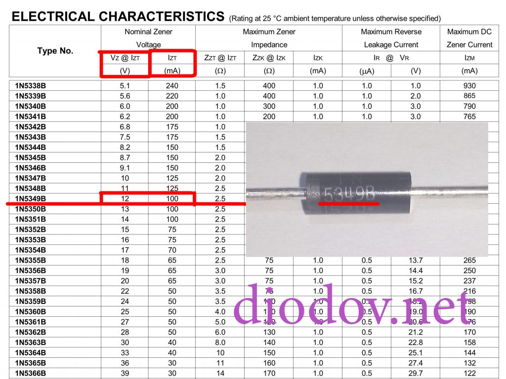
Менее понятный способ маркировки состоит из четырех цифр и буквы в конце. Если вы не опытный радиолюбитель, то без даташита никак не обойтись. Для примера расшифруем параметры опорного диода серии 1N5349B. Больше всего нас интересует первый столбец, в котором приведено номинальное напряжение 12 В. Второй столбец – номинальное значения ток – 100 мА.
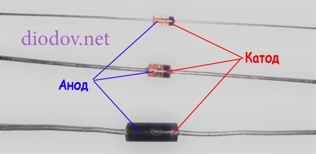
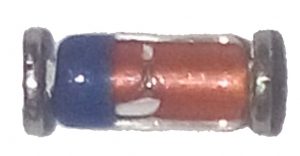
Катод стабилитрона любого типа обозначается кольцом черного или синего цвета, которое наносится на корпус со стороны соответствующего вывода.
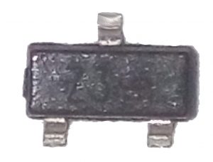
Маркировка SMD стабилитронов
Наибольшее распространение получили опорные диоды в стеклянном корпусе и в пластмассовом корпусе с тремя выводами. Маркировка SMD стабилитрона в стеклянном корпусе состоит из цветного кольца, цвет которого обозначает параметры данного полупроводникового прибора.
Если вам встретился SMD стабилитрон с тремя выводами, то следует знать, что один вывод – это «пустышка», то есть он не задействован и применяется лишь для надежной фиксации элемента на печатной плате после пайки. Анод и катод такого экземпляра проще всего определить с помощью мультиметра.
Мощность рассеивания стабилитрона
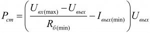
Мощность рассеивания стабилитрона Pст характеризует его способность не перегреваться выше определенной температуры на протяжении длительного времени. Чем выше значение Pст, тем больше тепла способен рассеять полупроводниковый прибор. Мощность рассеивания рассчитывается для самых неблагоприятных условий работы прибора, поэтому в ниже приведенную формулу подставляют максимально возможное в работе Uвх и наименьшие значения Rб и Iн:
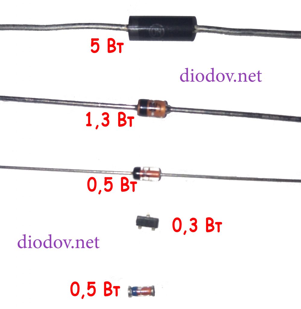
Существует ряд стандартных номиналом по данному параметру: 0,3 Вт, 0,5 Вт, 1,3 Вт, 5 Вт и т.п. Чем больше Pст, тем больше габариты полупроводникового прибора.
Как проверить стабилитрон
Проверить стабилитрон на предмет исправности довольно просто и быстро можно с помощью простейшего мультиметра. Для этого мультиметр следует перевести в режим «прозвонка», как правило, обозначенный знаком диода. Затем, если положительным щупом мультиметра прикоснуться анода, а отрицательным – катода, то на дисплее измерительного прибора мы увидим некоторое значение падения напряжения на pn-переходе. Поскольку к полупроводниковому прибору приложено прямое напряжение (смотрите прямую ветвь вольт-амперной характеристики), то опорный диод откроется.
Теперь, если щупы мультиметра поменять местами, тем самым приложить к выводам полупроводникового прибора обратное напряжение (смотрите обратную ветвь ВАХ), то он окажется заперт и не будет проводить ток. На дисплее измерительного прибора отобразится единица, обозначающая бесконечно высокое сопротивление.
Если в обеих случаях мультиметр покажет единицу или будет звенеть, то стабилитрон непригоден.
Еще статьи по данной теме
Диод. Светодиод. Стабилитрон / Хабр
Не влезай. Убьет! (с)
Постараюсь объяснить работу с диодами, светодиодами, а также стабилитронами на пальцах. Опытные электронщики могут пропустить статью, поскольку ничего нового для себя не обнаружат. Не буду вдаваться в теорию электронно-дырочной проводимости pn-перехода. Я считаю, что такой подход обучения только запутает начинающих. Это голая теория, почти не имеющая отношения к практике. Впрочем, интересующимся теорией предлагаю эту статью. Всем желающим добро пожаловать под кат.
Это вторая статья из цикла электроники. Рекомендую к прочтению также первую, которая повествует о том, что такое электрический ток и напряжение.
Диод – полупроводниковый прибор, имеющий 2 вывода для подключения. Изготавливается, упрощенно говоря, путем соединения 2х полупроводников с разным типом примеси, их называют донорной и акцепторной, n и p соответственно, поэтому диод содержит внутри pn-переход. Выводы, обычно состоящие из луженой меди, называют анод (А) и катод (К). Эти термины пошли еще со времен электронных ламп и используются в письменном виде, для обозначения направленности диода. Гораздо проще графическое обозначение. Названия выводов диода запомнятся сами собой при применении на практике.
Как я уже писал, мы не будем использовать теорию электронно-дырочной проводимости диода. Просто инкапсулируем эту теорию до черного ящика с двумя зажимами для подключения. Примерно так же программисты инкапсулируют работу со сторонними библиотеками, не вдаваясь в е… подробности их работы. Или, например, когда, пользуясь пылесосом, мы не вдаёмся в подробности, как он устроен внутри, он просто работает и нам важно одно из свойств пылесоса – сосать пыль.
Рассмотрим свойства диода, самые очевидные:
- От анода к катоду, такое направление называется прямым, диод пропускает ток.
- От катода к аноду, в обратном направлении, диод ток не пропускает. (Вообще-то нет. Но об этом позже.)
- При протекании тока, в прямом направлении, на диоде падает некоторое напряжение.
Возможно эти свойства вам и так хорошо известны. Но есть некоторые дополнения. Что же считать прямым, а что обратным направлением? Прямым называют такое включение, когда на аноде напряжение больше, чем на катоде. Обратное, наоборот. Прямое и обратное включение – это условность. В реальных схемах напряжение на одном и том же диоде может меняться с прямого на обратное и наоборот.
Кремниевый диод начинает пропускать хоть какой-либо значимый ток только тогда, когда на аноде напряжение будет больше примерно на 0,65 В, чем на катоде. Нет, не так. При протекании хоть какого-либо тока, на диоде образуется падение напряжения, примерно равное 0,65 В и выше.
Напряжение 0,65 В – называют прямым падением напряжения на pn-переходе. Это лишь примерная средняя величина, она зависит от тока, температуры кристалла и технологии изготовления диода. При изменении протекающего тока, она изменяется нелинейно. Чтобы как-то обозначить эту нелинейность графически, производители снимают вольтамперные характеристики диода. В мощных высоковольтных диодах падение напряжения может быть больше в 2, 3 и т.д. раза. Это означает, что внутри диода включено несколько pn-переходов последовательно.
Для определения падения напряжения можно использовать вольтамперную характеристику (ВАХ) диода в виде графика. Иногда эти графики приводятся в дата-листах (datasheets) на реальные модели диода, но чаще их нет. На первом мне попавшемся графике ниже приведены ВАХ КД243А, хотя это не важно, они все примерно похожи.
На графике Uпр – это прямое падение напряжения на диоде. Iпр – протекающий через диод ток. График показывает какое падение напряжения на диоде будет, при протекании n-го тока. Но чаще всего в даталистах не показываются реальные ВАХ, а приводится прямое падение напряжения, указанное при определенном токе. В английской литературе падение напряжения обозначается как forward voltage.
Как применять
Падение напряжения на диоде – для нас плохая характеристика, поскольку это напряжение не совершает полезной работы и рассеивается в виде тепла на корпусе диода. Чем меньше падение, тем лучше. Обычно падение напряжения на диоде определяют исходя из тока, протекающего через диод. Например, включим диод последовательно с нагрузкой. По сути это будет защита схемы от переплюсовки, на случай, если блок питания отсоединяемый. На рисунке ниже в качестве защищаемой схемы взят резистор 47 Ом, хотя в реальности это может быть все, что угодно, например, участок большой схемы. В качестве блока питания – батарея на 12 В.
Допустим, нагрузка без диода потребляет 255 мА. В данном случае это можно посчитать по закону Ома: I= U / R = 12 / 47 = 0,255 А или 255 мА. Хотя обычно потребление сферической схемы в вакууме уже известно, хотя бы по максимальным характеристикам блока питания. Найдем на графике ВАХ, указанный выше, падение напряжения для диода КД243А при 0,255 А протекающего тока, при 25 градусах. Оно равно примерно 0,75 В. Эти 0,75 В упадут на диоде, и для питания схемы останется 12 — 0,75 = 11,25 В — иногда может и не хватить. Как бонус, можно найти мощность, в виде тепла и потерь выделяющуюся на диоде по формуле P = I * U = 0,75 * 0,255 = 0,19 Вт, где I и U – ток через диод и падение напряжения на диоде.
Что же делать, когда график ВАХ недоступен? Например, для популярного диода 1n4007 указано только прямое напряжения forward voltage 1 В при токе 1 А. Нужно и использовать это значение, либо измерить реальное падение. А если для какого-либо диода это значение не указано, то сойдет среднее 0,65 В. В реальности проще это падение напряжения измерить вольтметром в схеме, чем выискивать в графиках. Думаю, не надо объяснять, что вольтметр должен быть включен на постоянное напряжение, если через диод течет постоянный ток, а щупы должны касаться анода и катода диода.
Немного про другие характеристики
В предыдущем примере, если перевернуть батарейку, я имею ввиду поменять полярность, см. нижний рисунок, ток не потечет и падение напряжения на диоде в худшем случае составит 12 В — напряжение батареи. Главное, чтобы это напряжение не превышало напряжение пробоя нашего диода, оно же обратное напряжение, оно же breakdown voltage. А также важно еще одно условие: ток в прямом направлении через диод не превышал номинальный ток диода, он же forward current. Это два основных параметра по которых выбирается диод: прямой ток и обратное напряжение.
Иногда в даталистах также указывается рассеиваемая мощность диодом или номинальная мощность (power dissipation). Если она указана, то ее нельзя превышать. Как ее посчитать, мы уже разобрались на предыдущем примере. Но если мощность не указана, тогда надо ориентироваться по току.
Говорят, что в обратном направлении ток через диод не течет, ну или почти не потечет. На самом деле через него протекает ток утечки, reverse current в английской литературе. Этот ток очень маленький, от нескольких наноампер у маломощных диодов до нескольких сот микроампер, у мощных. Также этот ток зависит от температуры и приложенного напряжения. В большинстве случаем ток утечки не играет никакой роли, например, в как в предыдущем примере, но, когда вы будете работать с наноамперами и поставите какой-либо защитный диод на входе операционного усилителя, тогда может случиться ой… Схема поведет себя совсем не так, как задумывалась.
У диодов так же есть некоторая маленькая паразитная емкость capacitance. Т.е., по сути, это конденсатор, параллельно включенный с диодом. Эту емкость надо учитывать при быстрых процессах при работе диода в схеме с десятками-сотнями мегагерц.
Также несколько слов по поводу термина «номинал». Обычно номинальные ток и напряжение обозначают, что при превышении этих параметров производитель не гарантирует работу изделия, если не сказано другое. И это для всех электронных компонентов, а не только для диода.
Что еще можно сделать
Применений диодов существует множество. Разработчики-радиоэлектронщики обычно выдумывают свои схемы из кусочков других схем, так называемых строительных кирпичиков. Вот несколько вариантов.
Например, схема защиты цифровых или аналоговых входов от перенапряжения:
Диоды в этой схеме при нормальной работе не пропускают ток. Только ток утечки. Но когда по входу возникает перенапряжение с положительной полуволной, т.е. напряжение входа становится больше чем Uпит плюс прямое падение напряжения на диоде, то верхний диод открывается и вход замыкается на шину питания. Если возникает отрицательная полуволна напряжения, то открывается нижний диод и вход замыкается на землю. В этой схеме, кстати, чем меньше утечки и емкость у диодов, тем лучше. Такие схемы защиты уже, как правило, стоят во всех современных цифровых микросхемах внутри кристалла. А внешними мощными сборками TVS-диодов защищают, например, USB порты на материнских платах.
Также из диодов можно собрать выпрямитель. Это очень распространённый тип схем и вряд ли кто-то из читателей про них не слышал. Выпрямители бывают однополупериодные, двухполупериодные и мостовые. С однополупериодным выпрямителем мы уже познакомились в нашем самом первом многострадальном примере, когда рассматривали защиту от переплюсовки. Никакими особыми плюсами не обладает, кроме плюса на батарейке. Один из самых важных минусов, который ограничивает применение схемы однополупериодного выпрямителя на практике: схема работает только с положительной полуволной напряжения. Отрицательное напряжение напрочь отсекает и ток при этом не течет. «Ну и что?», скажете вы, «Такой мощности мне будет достаточно!». Но нет, если такой выпрямитель стоит после трансформатора, то ток будет протекать только в одну сторону через обмотки трансформатора и, таким образом, трансформаторное железо будет дополнительно подмагничиваться. Трансформатор может войти в насыщение и греться намного больше положенного.
Двухполупериодные выпрямители этого недостатка лишены, но им необходим средний вывод обмотки трансформатора. Здесь при положительной полярности переменного напряжения открыт верхний диод, а при отрицательной – нижний. КПД трансформатора используется не полностью.
Мостовые схемы лишены обоих недостатков. Но теперь на пути тока включены два диода в любой момент времени: прямой диод и обратный. Падение напряжения на диодах удваивается и составляет не 0,65-1В, а в среднем 1,3-2В. С учетом этого падения считается выпрямленное напряжение.
Например, нам надо получить 18 вольт выпрямленного напряжения, какой трансформатор для этого выбрать? 18 вольт плюс падение на диодах, возьмем среднее 1,4 В, равно 19,4 В. Мы знаем из предыдущей статьи, что амплитудное значение переменного напряжения в корень из 2 раз больше его действующего значения. Поэтому во вторичной цепи трансформатора переменное действующее напряжение равно 19,4 / 1,41 = 13,75В. С учетом того, что напряжение в сети может гулять на 10%, а также под нагрузкой напряжение немного просядет, выберем трансформатор 230/15 В.
Мощность требуемого нам трансформатора можно посчитать от тока нагрузки. Например, мы собираемся подключать к трансформатору нагрузку в один ампер. Это если с запасом. Всегда оставляйте небольшой запас, в 20-40%. Просто по формуле мощности можно найти P = U * I = 15 * 1 = 15 ВА, где U и I – напряжение и ток вторичной обмотки. Если вторичных обмоток несколько, то их мощности складываются. Плюс потери на трансформацию, плюс запас, поэтому выберем трансформатор 20-40 ВА. Хотя часто трансформаторы продаются с указанием тока вторичных обмоток, но проверить по габаритной мощности не помешает.
После выпрямительного моста необходим сглаживающий конденсатор, на рисунке не показан. Не забывайте про него! Есть умные формулы по расчету этого конденсатора в зависимости от количества пульсаций, но порекомендую такое правило: ставить конденсатор 10000мкФ на один ампер потребления тока. Вольтаж конденсатора не меньше, чем выпрямленное без нагрузки напряжение. В данном примере можно взять конденсатор с номиналом 25В.
Диоды в этой схеме выберем на ток >=1А и обратное напряжение, с запасом, больше 19,4 В, например, 50-1000 В. Можно применить диоды Шоттки. Это те же диоды, только с очень маленьким падением напряжения, которое часто составляет десятки милливольт. Но недостаток диодов Шоттки – их не выпускают на более-менее высокие напряжения, больше 100В. Точнее с недавнего времени выпускают, но их стоимость заоблачная, а плюсы уже не так очевидны.
Светодиод
Внутри устроен совсем по другому, чем диод, но имеет те же самые свойства. Только еще и светится при протекании тока в прямом направлении.
Все отличие от диода в некоторых характеристиках. Самое важное – прямое падение напряжения. Оно гораздо больше, чем 0,65 В у обычного диода и зависит в основном от цвета светодиода. Начиная от красного, падение напряжения которого составляет в среднем 1,8 В, и заканчивая белым или синим светодиодом, падение у которых около 3,5 В. Впрочем, у невидимого спектра эти значения шире.
По сути падение напряжения здесь – минимальное напряжение зажигания диода. При меньшем напряжении, у источника питания, тока не будет и диод просто не загорится. У мощных осветительных светодиодов падение напряжения может составлять десятки вольт, но это значит лишь, что внутри кристалла много последовательно-параллельных сборок диодов.
Но сейчас поговорим об индикаторных светодиодах, как наиболее простых. Их выпускают в различных корпусах, наиболее часто в полуокруглых, диаметром 3, 5, 10 мм.
Любой диод светится в зависимости от протекающего тока. По сути это токовый прибор. Падение напряжения получается автоматически. Ток мы задаем сами. Современные индикаторные диоды более-менее начинают светиться при токе 1 мА, а при 10 мА уже выжигают глаза. Для мощных осветительных диодов надо смотреть документацию.
Применение светодиода
Имея лишь соответствующий резистор можно задать нужный ток через диод. Конечно, понадобится еще и блок питания постоянного напряжения, например, батарейка 4,5 В или любой другой БП.
Например, зададим ток 1мА через красный светодиод с падением напряжения 1,8 В.
На схеме показаны узловые потенциалы, т.е. напряжения относительно нуля. В каком направлении включать светодиод нам подскажет лучше всего мультиметр в режиме прозвонки, поскольку иногда попадаются напрочь китайские светодиоды с перепутанными ногами. При касании щупов мультиметра, в правильном направлении, светодиод должен слабо светиться.
Поскольку применен красный светодиод, то на резисторе упадет 4,5 — 1,8 = 2,7В. Это известно по второму закону Кирхгофа: сумма падений напряжения на последовательных участках схемы равно ЭДС батарейки, т.е. 2,7 + 1,8 = 4,5В. Чтобы ограничить ток в 1мА, резистор по закону Ома должен обладать сопротивлением R = U / I = 2,7 / 0,001 = 2700 Ом, где U и I – напряжение на резисторе и необходимый нам ток. Не забываем переводить величины в единицы СИ, в амперы и вольты. Поскольку выпускаемые номиналы сопротивлений стандартизованы выберем ближайший стандартный номинал 3,3кОм. Конечно, при этом ток изменится и его можно пересчитать по закону Ома I = U / R. Но зачастую это не принципиально.
В этом примере ток, отдаваемый батарейкой, мал, так что внутренним сопротивлением батареи можно пренебречь.
С осветительными светодиодами все тоже самое, только токи и напряжения выше. Но иногда им уже не требуется резистор, надо смотреть документацию.
Что-то еще про светодиод
По сути, светить – это основное назначение светодиода. Но есть и другое применение. Например, светодиод может выступать в качестве источника опорного напряжения. Они необходимы, например, для получения источников тока. В качестве источников опорного напряжения, как менее шумные, применяют красные светодиоды. Их включают в схему так же, как и в предыдущем примере. Поскольку напряжение батарейки относительно постоянное, ток через резистор и светодиод тоже постоянный, поэтому падение напряжения остается постоянным. От анода светодиода, где 1,8В, делается отвод и используется это опорное напряжение в других участках схемы.
Для более надежной стабилизации тока на светодиоде, при пульсирующем напряжении источника питания, вместо резистора в схему ставят источник тока. Но источники тока и источники опорного напряжения – это тема еще одной статьи. Возможно, когда-нибудь я ее напишу.
Стабилитрон
В английской литературе стабилитрон называется Zener diode. Все тоже самое, что и диод, в прямом включении. Но сейчас поговорим только про обратное включение. В обратном включении под действием определенного напряжения на стабилитроне возникает обратимый пробой, т.е. начинает течь ток. Этот пробой полностью штатный и рабочий режим стабилитрона, в отличие от диода, где при достижении номинального обратного напряжения диод просто выходил из строя. При этом, ток через стабилитрон в режиме пробоя может меняться, а падение напряжение на стабилитроне остается практически неизменным.
Что нам это дает? По сути это маломощный стабилизатор напряжения. Стабилитрон имеет все те же характеристики, что и диод, плюс добавляется так же напряжение стабилизации Uст или nominal zener voltage. Оно указывается при определенном токе стабилизации Iст или test current. Также в документации на стабилитроны указываются минимальный и максимальный ток стабилизации. При изменении тока от минимального до максимального, напряжение стабилизации несколько плавает, но незначительно. См. вольт-амперные характеристики.
Рабочая зона стабилитрона обозначена зеленым цветом. На рисунке видно, что напряжение на рабочей зоне практически неизменно, при широком диапазоне изменения тока через стабилитрон.
Чтобы выйти на рабочую зону, нам надо установить ток стабилитрона между [Iст. min – Iст. max] с помощью резистора точно так же, как это делалось в примере со светодиодом (кстати, можно также с помощью источника тока). Только, в отличие от светодиода, стабилитрон включен в обратном направлении.
При меньшем токе, чем Iст. min стабилитрон не откроется, а при большем, чем Iст. max – возникнет необратимый тепловой пробой, т.е. стабилитрон просто сгорит.
Расчёт стабилитрона
Рассмотрим на примере нашего рассчитанного трансформаторного БП. У нас есть блок питания, выдающий минимум 18 В (по сути там больше, из-за трансформатора 230/15 В, лучше мерить в реальной схеме, но суть сейчас не в этом), способный отдавать ток 1 А. Нужно запитать нагрузку с максимальным потреблением 50 мА стабилизированным напряжением 15 В (например, пусть это будет какой-нибудь абстрактный операционный усилитель – ОУ, у них примерно такое потребление).
Такая слабая нагрузка выбрана неспроста. Стабилитроны довольно маломощные стабилизаторы. Они должны проектироваться так, чтобы через них мог проходить без перегрева весь ток нагрузки плюс минимальный ток стабилизации Iст. min. Это необходимо, потому что ток после резистора R1 делится между стабилитроном и нагрузкой. В нагрузке ток может быть непостоянным, либо нагрузка может выключаться из схемы совсем. По сути это параллельный стабилизатор, т.е. весь ток, который не уйдет в нагрузку, примет на себя стабилитрон. Это как первый закон Кирхгофа I = I1 + I2, только здесь I = Iнагр + Iст. min.
Итак, выберем стабилитрон с напряжением стабилизации 15 В. Для установки тока через стабилитрон всегда необходим резистор (или источник тока). На резисторе R1 упадет 18 – 15 = 3 В. Через резистор R1 будет протекать ток Iнагр. + Iст. min. Примем Iст. min = 5 мА, это примерно достаточный ток для всех стабилитронов с напряжением стабилизации до 100 В. Выше 100 В можно принимать 1мА и меньше. Можно взять Iст. min и больше, но это только будет бесполезно греть стабилитрон.
Итак, через R1 течет Ir1 = Iнагр. + Iст. min = 50 + 5 = 55 мА. По закону Ома находим сопротивление R1 = U / I = 3 / 0,055 = 54,5 Ом, где U и I – напряжение на резисторе и ток через резистор. Выберем из ближайшего стандартного ряда сопротивление 47 Ом, будет чуть больше ток через стабилитрон, но ничего страшного. Его даже можно посчитать, общий ток: Ir1 = U / R = 3 / 47 = 0,063А, далее минимальный ток стабилитрона: 63 — 50 = 13 мА. Мощность резистора R1: P = U * I = 3 * 0,063 = 0,189 Вт. Выберем стандартный резистор на 0,5 Вт. Советую, кстати, не превышать мощность резисторов примерно Pmax/2, дольше проживут.
На стабилитроне тоже рассеивается мощность в виде тепла, при этом в самом худшем случае она будет равна P = Uст * (Iнагр + Iст.) = 15 * (0,050 + 0,013) = 0,945 Вт. Стабилитроны выпускают на разную мощность, ближайшая 1Вт, но тогда температура корпуса при потреблении около 1Вт будет где-то 125 градусов С, лучше взять с запасом, на 3 Вт. Стабилитроны выпускают на 0,25, 0,5, 1, 3, 5 Вт и т.д.
Первый же запрос в гугле «стабилитрон 3Вт 15В» выдал 1N5929BG. Далее ищем «datasheet 1N5929BG». По даташиту у него минимальный ток стабилизации 0,25 мА, что меньше 13 мА, а максимальный ток 100 мА, что больше 63 мА, т.е. укладывается в его рабочий режим, поэтому он нам подходит.
В общем-то, это весь расчёт. Да, стабилизатор это неидеальный, внутреннее сопротивление у него не нулевое, но он простой и дешевый и работает гарантировано в указанном диапазоне токов. А также поскольку это параллельный стабилизатор, то ток блока питания будет постоянным. Более мощные стабилизаторы можно получить, умощнив стабилитрон транзистором, но это уже тема следующей статьи, про транзисторы.
Проверить стабилитрон на пробой обычным мультиметром, как правило, нельзя. При более-менее высоковольтном стабилитроне просто не хватит напряжения на щупах. Единственное, что удастся сделать, это прозвонить его на наличие обычной диодной проводимости в прямом направлении. Но это косвенно гарантирует работоспособность прибора.
Еще стабилитроны можно использовать как источники опорного напряжения, но они шумные. Для этих целей выпускают специальные малошумящие стабилитроны, но их цена в моем понимании зашкаливает за кусочек кремния, лучше немного добавить и купить интегральный источник с лучшими параметрами.
Также существует много полупроводниковых приборов, похожих на диод: тиристор (управляемый диод), симистор (симметричный тиристор), динистор (открываемый импульсно только по достижении определенного напряжения), варикап (с изменяемой емкостью), что-то еще. Первые вам понадобятся в силовой электронике при постройки управляемых выпрямителей или регуляторов активной нагрузки. А с последними я уже лет 10 не сталкивался, поэтому оставляю эту тему для самостоятельного чтения в вики, хотя бы про тиристор.
90000 How to Define Anode and Cathode 90001 How to Define Anode and Cathode 90002 How to Define Anode and Cathode 90003 90004 John Denker 90005 90006 90007 * Contents 90008 90007 1 Definition 90008 90011 90012 Definition: The 90004 anode 90005 of a device is the terminal where current flows in from outside. The 90004 cathode 90005 of a device is the terminal where current flows out. This is illustrated in figure ~ 1. 90002 A useful mnemonic is ACID: Anode Current Into Device.By current we mean the positive conventional current. Since electrons are negatively charged, positive current flowing in is the same as electrons flowing out. 90006 90002 That’s essentially all there is to it. 90006 90021 90022 90007 2 Some Examples 90008 90002 Our definition applies easily and correctly to every situation I can think of (with one execrable exception, as discussed item 11 below). 90006 90027 90012 Voltaic cells and batteries. 90021 90012 The hot cathode in a cathode-ray tube, as found in an old-style television or oscilloscope.90021 90012 The hot cathode in an electronic amplifier tube ( «Fleming valve «). 90021 90012 The hot cathode in an X-ray tube, as in figure ~ 2. 90021 90012 The rotating anode in an X-ray tube, as in figure ~ 2. 90021 90012 A common-anode LED array, such as a 7-segment digit array, although this is not optimal terminology, for reasons discussed in item 8. 90021 90012 The sacrificial anode in a boat; see item 16. 90021 90012 The anode plate and cathode plate (as well as anode mud) in an electrolytic refining cell; see item 9.90021 90044 90002 Crucially, our definition applies just fine to things like a rechargeable battery, where you can not identify the anode and cathode until you see how the device is being operated, as discussed in item 6. 90006 90002 Our definition also applies just fine in cases where it is relatively easy to distinguish anode from cathode «just by looking» as discussed in item 7. 90006 90002 There is one execrable exception, as discussed item 11 below. 90006 90007 3 Discussion 90008 90053 90054 90055 Ours is the original, time-honored definition.It is consistent with the etymology, as discussed in item 17. There is no other sensible definition. I’ve seen several attempts at definitions, but unless they were equivalent to our definition (as given in section ~ 1), they were grotesquely overcomplicated, wrong, or both. 90056 90054 90055 By well-established convention (going back to Ben Franklin), when we speak of 90004 current 90005 we mean the conventional positive current. In metal wires, the current is carried by 90004 electrons 90005 moving in the direction opposite to the current.This complicates the notion of current, but is necessary because the electron is negatively charged. 90056 90054 90055 For the vast majority of people, there is no point in memorizing the meaning of anode and cathode. The terms just are not very useful, unless you get a job in an electrochemistry laboratory or some comparably narrow specialty. If some day you do need to know the meanings, you can look them up that morning and forget them again that evening. 90056 90054 90055 Note that when we say current-in, we mean current flowing into the device from the external circuit.Similarly when we say current-out, we mean current flowing out of the device toward the external circuit. We are treating the device as a black box, and we are emphatically not talking about whatever currents flow within the device. This black-box terminology is standard in all branches of engineering and science, unless the context clearly requires otherwise. 90002 If you insist on peeking inside the black box, the story gets more complicated, as you can see in figure ~ 2. However, this does not change the letter or the spirit of the definition, which is based on the behavior of the black box, as seen from the outside.90006 90056 90054 90055 It is crucial to remember that the anode / cathode distinction is based on current, not voltage. Anode / cathode is not the same as positive / negative or vice versa. Illustrative example: for a battery being discharged, the positive terminal is the cathode, while for the same battery being recharged, the positive terminal is the anode. 90056 90054 90055 As a trustworthy rule, keep in mind that anode and cathode refer to function, not structure. There are lots of devices where it would be madness to permanently label the structures as anode or cathode, because their function changes from time to time.Rechargeable batteries are a common, very important example, as mentioned in item 5. 90056 90054 90055 Although anode and cathode are fundamentally defined in terms of 90004 function 90005 not structure, there are some exceptional devices where the function is essentially locked to the structure. In such a case, it is arguably permissible to label the 90004 structures 90005 as anode and cathode, because only one direction of current-flow makes sense. On the list in section ~ 2, all the examples 90004 except for the rechargeable battery 90005 are in this category.90002 In any case, keep in mind that this category must be considered the risky exception, not the general rule. The trusty general rule is explained in item 6. 90006 90056 90054 90055 Even in cases where it is arguably possible to identify a definite anode and cathode, there are usually simpler and better ways to designate the terminals. Specifically, for a battery (rechargeable or not), it is conventional and sensible to speak of the positive terminal and negative terminal. For a diode, it is conventional and sensible to speak of the P-doped side and the N-doped side.In particular, for a LED display module, the so-called common-anode configuration would more properly be called the common-P-side configuration. 90056 90054 90055 Here’s an interesting and important example: Consider the electrolytic refining of metals such as copper. 90002 During normal operation, a large current flows through the cell, imposed from the outside. Current is pushed into the cell at the anode, and taken out at the cathode. The terminals are labeled according to their normal function, in accordance with the definition given in section ~ 1.90006 90002 At the beginning of the operation, the anode is impure copper. At the end of the operation, the cathode is much higher purity copper. Try googling for anode mud. 90006 90002 If some wise guy temporarily reversed the direction of the current, the normal anode would become the temporary cathode and vice versa. However, this possibility is so kooky that it is usually not even considered. The terminals are labeled according to their 90004 normal 90005 function. 90006 90002 Note the contrast: 90006 90104 90105 90106 90107 Electrolytic refining cell.90108 90109 90110 90109 90106 90107 Ordinary battery 90108 90109 90116 90117 90104 90105 90106 In the refining cell, the open-circuit cell voltage, if any, is very small and completely irrelevant. 90109 90110 90109 90106 In the battery, there is a definite positive terminal and a definite negative terminal. 90109 90116 90117 90104 90105 90106 The voltage drop across the cell is roughly proportional to the current. During operation, the anode will be at a positive voltage relative to the cathode.90109 90110 90109 90106 The voltage drop across the cell is qualitatively the same, no matter whether the current is positive, negative, or zero. The positive terminal is the cathode during discharge, but it is the anode during recharge. 90109 90116 90117 90056 90054 90055 In all cases, you can use the descriptive terms current-sink and current-source as synonyms for anode and cathode. Description is generally preferable to jargon. 90056 90054 90055 It is possible to buy an array of Zener diodes.Alas, according to an established but illogical convention, the so-called common-anode configuration is structurally analogous to a common-anode array of LEDs, in the sense that the P-doped sides are tied together. This is an abomination, because in normal Zener usage, the P-doped side is where the current exits, and should logically be called the cathode. Apparently somebody was under the misimpression that anode / cathode referred to structure instead of function. 90002 You should never use the terms anode or cathode to describe the structural parts of a Zener diode, for the same reason you should not use such terms for the structure of a rechargeable battery.Anode and cathode refer to function, not structure. Instead you should refer to the P-doped side and the N-doped side, and you should insist that others do the same. 90006 90002 Note that reversing the labeling convention for Zener diode arrays would not solve the problem in any fundamental sense, because there are perfectly reasonable circuits in which — part of the time — a Zener diode is forward biased, so that it conducts just like any other diode. This is the same situation we encounter in connection with rechargeable batteries: if you attach permanent anode / cathode labels to the structure, you will be wrong at least part of the time.90006 90148 90105 90150 90148 90105 90150 90148 90105 90150 The terms «anode» and «cathode» 90003 properly apply to function, not structure. 90109 90116 90117 90109 90116 90117 90109 90150 ~~~~~ 90109 90116 90117 90056 90054 90055 Electrochemical corollary: In any electrochemical cell, oxidation reactions take place at the anode, and reduction reactions take place at the cathode. (If you do not know what this means, do not worry about it.) This includes batteries being charged (Anode = positive) as well as batteries being discharged (Anode = negative).This is a corollary flowing from our definition, and from the conventional viewpoint that the cell is the black box, and everything external to the cell is the external circuit. 90002 The situation is summarized in the following table: 90006 90148 90105 90150 ~ 90109 90150 ~~~~~ 90109 90150 90107 charging 90108 90109 90150 ~~~~~ 90109 90150 90107 discharging 90108 90109 90116 90105 90150 ~~~ 90109 90150 ~~~~~ 90109 90116 90105 90150 — plate: 90109 90150 ~~~~~ 90109 90150 cathode 90003 being reduced 90109 90150 ~~~~~ 90109 90150 anode 90003 being oxidized 90109 90116 90105 90150 ~~~ 90109 90150 ~~~~~ 90109 90116 90105 90150 + plate: 90109 90150 ~~~~~ 90109 90150 anode 90003 being oxidized 90109 90150 ~~~~~ 90109 90150 cathode 90003 being reduced 90109 90116 90117 90056 90054 90055 Let us make a brief exception to the black-box viewpoint, and consider what happens inside an electrochemical cell.Inside the cell, cations (positively charged species) moving toward the cathode make a positive contribution to the conventional current 90004 inside the cell 90005, as shown in figure ~ 3. Similarly, anions (negatively charged species) moving toward the anode make a positive contribution to the conventional current 90004 inside the cell 90005. No anions are shown in the figure. The rule anions-to-anode, cations-to-cathode applies only inside the cell. This rule is required by the fact that current obeys a conservation law; current that flows into the cell at the anode must flow through the cell and then out the cathode.Outside the cell, current flows toward the anode; inside the cell, current flows away from the anode. (By the way, it is usually assumed that outside the cell, there are no mobile anions or cations, just electrons carried by metal wires in the external circuit.) 90003 Figure ~ 3: Anode and Cathode: Inside the Black Box 90002 When talking about ions, you need to remember that cations are positively charged. The mnemonic for cations is to view the ‘t’ as a plus sign: ca + ion. Meanwhile, the mnemonic for anions is something of an acronym: A Negative ION = ANION.90006 90002 When remembering the cations-to-cathode rule, you need to remember that inside the cell, cations go to (not from) the cathode: ca + ions + O ca + hode. The corresponding anions-to-anode rule is equally valid, but you have to work harder to remember that the anions go to (Not from) the anode. 90006 90002 Please remember that the cations-to-cathode rule is subject to multiple caveats. It is at best a chemical corollary to the real definition. It can not possibly serve as the definition of cathode, because the cathode is well-defined for all sorts of devices that do not have any mobile cations, e.g. semiconductor diodes, cathode-ray tubes, et cetera. Another caveat is that this rule applies to what’s going on inside the cell, whereas for most purposes (including the anode / cathode definition) it is conventional and appropriate to focus on the properties of the black box, as seen from the outside. (Similar issues arise in item 14 and item 16.) 90006 90056 90054 90055 There is some slight potential for confusion when thinking about cathode ray tubes and X-ray tubes, because of the temptation to deviate from the black-box viewpoint.(Similar issues arise in item 13 and item 16.) In an X-ray tube, the interesting physics is happening inside the device, whereas the definition of anode is expressed in terms of conventional current flowing into the external terminal, flowing into the black box from outside. Remember, from outside the device we see positive conventional current coming out of the cathode and going into the anode, in accordance with our definition, as seen in figure ~ 1 in section ~ 1. The rule is ACID: Anode Current Into Device.(If we peek inside the device, we see electrons streaming out of the cathode, but that’s only a corollary of the definition, not the definition 90004 per se 90005.) 90056 90054 90055 There is even more potential for confusion if you try to explain or define anode / cathode in terms of electrochemical cells, if only because very very few people understand how such things work. See reference ~ 1 and references therein. As the saying goes, learning proceeds from the known to the unknown. Our definition of anode / cathode, as given in section ~ 1, is simple and useful.The internal mechanism of a battery is not simple. It makes no sense to «explain» the former in terms of the latter. 90002 Battery terminals are labeled positive and negative. They are labeled according to voltage, not charge or current. This is conventional and entirely appropriate, because the positive terminal remains at a positive voltage (relative to the other terminal) during all normal conditions, including when the battery is discharging, recharging, or just sitting there in equilibrium with no current flowing.90006 90002 In contrast, as mentioned in item 5, it would be wildly inappropriate to label the battery terminals as anode and cathode. That’s because the terminal that is the cathode during discharge becomes the anode during recharge … and is neither anode nor cathode in the equilibrium (no current) situation. 90006 90002 Furthermore, it makes no sense to define anode and cathode in terms of electrochemisty, because the terms are used in all sorts of situations where there is no electrochemistry involved, including semiconductor diodes, X-ray tubes, et cetera.90006 90056 90054 90055 Boats and other structures in contact with salt water give rise to a situation with some potential for confusion about anode versus cathode. At first glance it might not be obvious what’s considered the «black box» and what’s considered the «External circuit». The conventional viewpoint is this: 90011 90012 The water, and the metals touching the water, are to be thought of as a giant electrochemical cell. There are anions and cations in the water, inside the black box.90021 90012 The structure of the boat (or whatever) is considered the external circuit. There are no anions or cations. The current is carried by electrons flowing inside metals. 90021 90022 90002 That is to say, the convention is to consider the boat as external to the water … even though it might seem more logical to think of the water as external to the boat. This may seem arbitrary, but at least it is consistent with the aforementioned electrochemical corollary (Item 12), so that oxidation reactions take place at the anode, and reduction reactions take place at the cathode.This leads us to the useful concept of a 90004 sacrificial anode 90005, which is just a cheap, easily-replaceable electrode that is placed in the water and arranged to have a large positive voltage with respect to the rest of the boat. That makes everything else on the boat a cathode, greatly reducing corrosion, because most forms of corrosion involve oxidation reactions. To say the same thing in other words, inside the water, highly corrosive anions such as OH 90272 90272 — 90274 90274 and Cl 90272 90272 — 90274 90274 are flowing toward the anode and away from everything else, in accordance with the anions-to-anode rule.The anode, of course, corrodes rapidly, and needs to be replaced on occasion. 90006 90056 90054 90055 Etymology: The words anode and cathode were introduced in 1834 by Michael Faraday on the advice of William Whewell, the polymathic scientist and prolific wordsmith. Whewell understood quite a bit of Greek, and put it to good use: 90011 90012 Anode comes from the Greek roots ἀνά + ὀδός (meaning upward path). 90021 90012 Cathode comes from the Greek roots κατά + Ὀδός (meaning downward path).90021 90022 90002 One should never place too much emphasis on etymology, because meanings can drift over time. Indeed ἀνά and κατά have drifted from their ancient roots. However, ὀδός has not, and that’s the key. The English words, when coined, were clearly intended to describe flow, not voltage. The same roots are used in other Greek and pseudo-Greek terms in English, e.g. anabolic, cataract, odometer, et cetera. 90006 90056 90293 90007 4 Summary 90008 90002 I am astonished that some people take a concept that is simple and unimportant, make it needlessly complex, and pretend it is important.90006 90002 When dealing with batteries, do not think in terms of anode and cathode; think in terms of positive terminal and negative terminal. 90006 90002 When dealing with semiconductor diodes, do not worry about anode and cathode; think in terms of P-doped side and N-doped side. 90006 90002 The general rule is: Anode means current 90004 into 90005 the black box and cathode means current 90004 out from 90005 the black box. Zener diodes give rise to an execrable exception that should be avoided like the plague.90006 90002 There is abundant evidence that even people who call themselves experts can not keep the anode / cathode terminology straight. In any practical situation, there is always a way to figure out how to hook things up without a deep understanding of anode versus cathode. 90006 90002 The terms anode and cathode are sometimes convenient, in situations where only one direction of current makes sense. 90006 90002 In other situations, it is usually better to avoid the terms anode and cathode. There are better ways to say what needs to be said.Constructive suggestion: it is better to talk about the current (Rather than the electrode). It is better to talk about what the current is 90004 doing 90005 (rather than what the electrode «is»). 90006 90007 5 References 90008 90053 90319 90320 90055 John Denker, «How a Battery Works» 90003 www.av8n.com/physics/battery.htm 90056 90293 .90000 Polarity — learn.sparkfun.com 90001 Favorited Favorite 39 90002 What is Polarity? 90003 90004 In the realm of electronics, 90005 polarity 90006 indicates whether a circuit component is 90005 symmetric 90006 or not. A non-polarized component — a part 90009 without 90010 polarity — can be connected in any direction and still function the way it’s supposed to function. A symmetric component rarely has more than two terminals, and every terminal on the component is equivalent.You can connect a non-polarized component in any direction, and it’ll function just the same. 90011 90004 A 90005 polarized 90006 component — a part 90009 with 90010 polarity — can only be connected to a circuit in one direction. A polarized component might have two, twenty, or even two-hundred pins, and each one has a unique function and / or position. If a polarized component was connected to a circuit incorrectly, at best it will not work as intended. At worst, an incorrectly connected polarized component will smoke, spark, and be one very dead part.90011 90004 90009 An assortment of polarized components: batteries, integrated circuits, transistors, voltage regulators, electrolytic capacitors, and diodes, among others. 90010 90011 90004 Polarity is a very important concept, especially when it comes to physically building circuits. Whether you’re plugging parts into a breadboard, soldering them to a PCB, or sewing them into an e-textile project, it’s critical to be able to identify polarized components and to connect them in the correct direction.So that’s what we’re here for! In this tutorial we’ll discuss which components do and do not have polarity, how to identify component polarity, and how to test some components for polarity. 90011 90024 Consider Reading 90025 90004 If your head’s not swimming yet, it’s probably safe to read through the rest of this tutorial. Polarity is a concept which builds on some lower-level electronics concepts and reinforces a few others. If you have not already, consider checking out some of the below tutorials, before you read through this one.90011 90024 What is a Circuit? 90025 90004 Every electrical project starts with a circuit. Do not know what a circuit is? We’re here to help. 90011 90024 How to Use a Breadboard 90025 90004 Welcome to the wonderful world of breadboards. Here we will learn what a breadboard is and how to use one to build your very first circuit. 90011 90024 How to Use a Multimeter 90025 90004 Learn the basics of using a multimeter to measure continuity, voltage, resistance and current.90011 90002 Diode and LED Polarity 90003 90005 Note: 90006 We will be referring to the flow of current that is relative to the positive charges (i.e. conventional current) in a circuit. 90004 Diodes only allow current to flow in one direction, and they’re 90009 always 90010 polarized. A diode has two terminals. The positive side is called the 90009 anode 90010, and the negative one is called the 90009 cathode 90010. 90011 90004 90009 The diode circuit symbol, with the anode and cathode marked.90010 90011 90004 Current through a diode can only flow from the anode to the cathode, which would explain why it’s important for a diode to be connected in the correct direction. Physically, every diode should have some sort of indication for either the anode or cathode pin. Usually the diode will have a 90005 line near the cathode pin 90006, which matches the vertical line in the diode circuit symbol. 90011 90004 Below are a few examples of diodes. The top diode, a 1N4001 rectifier, has a grey ring near the cathode.Below that, a 1N4148 signal diode uses a black ring to mark the cathode. At the bottom are a couple surface mount diodes, each of which use a line to mark which pin is the cathode. 90011 90004 90009 Notice the lines on each device, denoting the Cathode side, which match the line in the symbol above. 90010 90011 90024 LEDs 90025 90004 LED stands for light-emitting 90009 diode 90010, which means that much like their diode cousins, they’re polarized. There are a handful of identifiers for finding the positive and negative pins on an LED.You can try to find the 90005 longer leg 90006, which should indicate the positive, anode pin. 90011 90004 Or, if someone’s trimmed the legs, try finding the flat edge on the LED’s outer casing. The pin nearest the 90005 flat edge 90006 will be the negative, cathode pin. 90011 90004 There might be other indicators as well. SMD diodes have a range of anode / cathode identifiers. Sometimes it’s easiest to just use a multimeter to test for polarity. Turn the multimeter to the diode setting (usually indicated by a diode symbol), and touch each probe to one of the LED terminals.If the LED lights up, the positive probe is touching the anode, and the negative probe is touching the cathode. If it does not light up, try swapping the probes around. 90011 90004 90009 The polarity of a tiny, yellow, surface-mount LED is tested with a multimeter. If the positive lead touches the anode and negative touches the cathode, the LED should light up. 90010 90011 90084 90004 Diodes certainly are not the only polarized component. There are tons of parts out there that will not work if connected incorrectly.Next we’ll discuss some of the other common polarized components, beginning with integrated circuits. 90011 90002 Integrated Circuit Polarity 90003 90004 Integrated circuits (ICs) might have eight pins or eighty pins, and each pin on an IC has a unique function and position. It’s very important to keep polarity straight with ICs. There’s a good chance they’ll smoke, melt, and be ruined if connected incorrectly. 90011 90004 Through-hole ICs usually come in a dual-inline package (DIP) — two rows of pins, each spaced by 0.1 «wide enough to straddle the center of a breadboard. DIP ICs usually have a 90005 notch 90006 to indicate which of the many pins is the first. If not a notch, the IC might have an etched 90005 dot 90006 in the casing near pin 1. 90011 90004 90009 An IC with both a dot and a notch to indicate polarity. Sometimes you get both, sometimes you only get one or the other. 90010 90011 90004 For all IC packages, pin numbers increase sequentially as you move counter-clockwise away from pin 1.90011 90004 Surface-mount ICs might come in QFN, SOIC, SSOP, or a number of other form-factors. These ICs will usually have a 90005 dot 90006 near pin 1. 90011 90009 An ATmega32U4 in a TQFP package, next to the datasheet pinout. 90010 90002 Electrolytic Capacitors 90003 90004 Not all capacitors are polarized, but when they are, it’s 90009 very 90010 important not to mix their polarity up. 90011 90004 Ceramic capacitors — the small (1μF and less), commonly yellow guys — are 90005 not 90006 polarized.You can stick those in either way. 90011 90009 Through-hole and SMD 0.1μF ceramic capacitors. These are NOT polarized. 90010 90004 Electrolytic caps (they’ve got electrolytes), which look like little tin cans, 90005 are polarized 90006. The negative pin of the cap is usually indicated by a 90005 «-» marking 90006, and / or a 90005 colored strip 90006 along the can. They might also have a 90005 longer positive leg 90006. 90011 90004 Below are 10μF (left) and a 1mF electrolytic capacitors, each of which has a dash symbol to mark the negative leg, as well as a longer positive leg.90011 90004 Applying a negative voltage for an extended period to an electrolytic capacitor results in a briefly exciting, but catastrophic, failure. They’ll make a 90009 pop 90010, and the top of the cap will either swell or burst open. From then on the cap will be as good as dead, acting like a short circuit. 90011 90002 Other Polarized Components 90003 90024 Batteries and Power Supplies 90025 90004 Getting polarity right in your circuit all starts and ends with getting the power supply connected correctly.Whether you’re project’s getting power from a wall-wart or a LiPo battery, it’s critical to make sure you do not accidently connect them backwards and apply 90005 — 90006 9V or 90005 — 90006 4.2V to your project accidently. 90011 90004 Anyone that’s ever replaced batteries knows how to find their polarity. Most batteries will indicate the positive and negative terminals with a «+» or «-» symbol. Other times it might be red wire for positive and a black wire for negative. 90011 90009 An assortment of batteries.Lithium polymer, coin cell, 9V alkaline, AA alkaline, and AA NiMH. Each has some way to represent positive or negative terminals. 90010 90004 Power supplies usually have a standardized connector, which should usually have polarity itself. A barrel jack, for example, has two conductors: outer and inner; the inner / center conductor is usually the positive terminal. Other connectors, like a JST, are 90005 keyed 90006 so you just can not connect them backwards. 90011 90004 For extra protection against reversing power supply polarity, you can add reverse polarity protection using a diode, or a MOSFET.90011 90024 Transistors, MOSFETs, and Voltage Regulators 90025 90004 These (traditionally) three-terminal, polarized components are lumped together because they share similar package types. Through-hole transistors, MOSFETs, and voltage regulators commonly come in a TO-92 or TO-220 package, seen below. To find which pin is which, look for the flat edge on the TO-92 package or the metal heatsink on the TO-220, and match that up to the pin-out in the datasheet. 90011 90009 Above, a 2N3904 transistor in a TO-92 package, note the curved and straight edges.A 3.3V regulator in a TO-220 package, note the metal heatsink on the back. 90010 90024 Etc. 90025 90004 This is just the tip of the polarized-component iceberg. Even non-polarized components, like resistors, can come in polarized packages. A resistor pack — a grouping of five-or-so pre-arranged resistors — is one such example. 90011 90009 A polarized resistor pack. An array of five 330 & ohm; resistors, all tied together at one end. The dot represents the first, common pin. 90010 90004 Fortunately, every polarized component should have some way to inform you which pin is which.Be sure to always 90005 read the datasheets 90006, and check the case for dots or other markers. 90011 90002 Resources and Going Further 90003 90004 Now that you know what polarity is, and how to identify it, why not check out some of these related tutorials: 90011 90177 90178 Connector Basics — There are a number of connectors which have polarity of their own. Usually this is a great way to make sure you do not apply power or some other signal backwards.90179 90178 Diodes — Our shining example of component polarity. This tutorial goes further in-depth on how diodes work, and what types of diodes are out there. 90179 90178 LilyPad Design Kit Experiment 1 — Circuits do not just exist on breadboards and circuit boards, you can sew them into shirts and other textiles too! Check out the LilyPad Design Kit tutorials to see how to get started. Knowing polarity will be huge in wiring up those LEDs correctly. 90179 90184 90004 90011 90004 90011 .90000 Diode operation — Energy Education 90001 90002 Figure 1. The p-n junction of a diode along with its corresponding schematic and real component. 90003 [1] 90004 The cathode and the anode of the diode are labelled so that conventional current flows from anode to cathode through the diode. 90005 The way that a 90006 diode operates 90007 can be difficult to understand as it involves fairly advanced quantum mechanics. However, at the simplest level the operation of a diode can be understood by looking at the flow of positive charges (or «holes») and the negative charges (the electrons).Technically, a semiconductor diode is referred to as a 90006 p-n junction 90007. These p-n junctions are important in the operation of a photovoltaic cell as well. Having the diode work properly requires a process known as doping. Semiconductors can be doped with materials so that they have an excess of easily displaced electrons — generally referred to as a 90006 negative 90007 or 90006 n-type 90007 region. As well, they can be doped with elements that create an excess of holes that easily absorb these electrons — generally referred to as a 90006 positive 90007 or 90006 p-type 90007 region.90003 [2] 90004 90003 [3] 90004 The negative and positive regions of the diode are also the component’s cathode and anode respectively (see Figure 1). 90022 90005 The differences between these two materials and their interactions over very short distances (less than a millimeter) result in a diode when the two types are joined. Joining these two types creates the p-n junction, and the region between the two sides is called the depletion region, as electrons from the n-type region diffuse and fill some of the holes in the p-type region.This creates negative ions in the p-type region and leaves behind positive ions in the n-type region (see Figure 2). 90003 [4] 90004 This responds to electric fields differently depending on the direction of the electric field. This leads to useful electronic behaviour depending on which way the voltage (or electric field) is applied, this is called biasing. 90022 90027 Bias 90028 90005 A diode (PN junction) in an electrical circuit allows current to flow more easily in one direction than another.Forward biasing means putting a voltage across a diode that allows current to flow easily, while reverse biasing means putting a voltage across a diode in the opposite direction. The voltage with reverse biasing does not cause any appreciable current to flow. This is useful for changing AC current to DC current. It has other uses in manipulating electronic signals as well. 90022 90031 Reverse Bias 90032 90033 90005 Figure 2. A reverse-biased p-n junction with the black circles representing easily displaced electrons and the white circles representing electron-deficient «holes.»In a reverse-biased junction such as this, the electrons would leave the black circles and move toward the external circuit, leaving behind more positive ions, while electrons from the external circuit would» fill the holes, «creating more negative ions. 90022 90005 If a voltage is applied across the diode in such a way that the n-type half of the diode was connected to the positive terminal of the voltage source and the p-type half was connected to the negative terminal, electrons from the external circuit would create more negative ions in the p-type region by «filling the holes» and more positive ions would be created in the n-type region as electrons are displaced toward the positive terminal of the voltage source (see Figure 2).Hence, the depletion region would increase and the voltage between the p-type and n-type regions would also increase as the total charge on each side of the junction increases in magnitude until the voltage across the diode equals and opposes the applied voltage and cancels it out, ceasing the current through the circuit. This process happens nearly instantaneously and results in essentially no current flow through the circuit when voltage is applied in this direction across the diode. This is known as a reverse-biased p-n junction.90003 [5] 90004 90022 90031 Forward Bias 90032 90042 90005 Figure 3. A partially and fully forward-biased p-n junction. Note that a minimum voltage is required to collapse the depleted region. 90022 90005 When the voltage is applied in the opposite direction across the diode, the depletion region begins to shrink (see Figure 3). In a reverse-biased diode, the electrons and holes would be pulled away from the junction, but a forward-biased scenario ensures that the electrons and holes move toward the junction as they are repelled from the positive and negative terminals of the voltage source respectively .90003 [1] 90004 90003 [6] 90004 Given a great enough applied voltage, both the holes and the electrons would overcome the depletion region and meet near the junction, where they could combine in a continuous process, closing the circuit and allowing current flow . 90022 90031 Forward Voltage and Breakdown Voltage 90032 90005 There is a minimum threshold voltage required to overcome the depletion region, which for most silicon diodes is a significant 0.7 volts. Furthermore, reverse-bias voltage does induce a small amount of current through the diode called leakage current that is essentially negligible for most purposes.Finally, a great enough reverse voltage will result in the complete electronic breakdown of the diode and allow current to flow through the diode in the reverse direction. 90003 [1] 90004 90022 90005 For more information about diodes, please see all about circuits or hyperphysics. 90022 90027 For Further Reading 90028 90005 For further information please see the related pages below: 90022 90027 References 90028 .90000 Types of Diodes and Their Applications 90001 90002 90003 Various Types Of Diodes With Their Characteristics & Uses 90004 90005 90006 The diode is the most used semiconductor device in electronics circuits. 90003 It is a two-terminal electrical check valve that allows the flow of current in one direction 90004. They are mostly made up of silicon but germanium is also used. Usually, they are used for rectification. But there are different properties & characteristics of diodes which can be used for different application.These characteristics are modified to form different types of diodes. Nowadays, several different types of diodes having different properties are available. 90009 90006 90011 90011 90009 90006 90009 90006 90017 Some of the different types of diodes with their properties and applications are discussed below: 90018 90009 90020 90003 P-N Junction Diode 90004 90023 90006 The P-N junction diode is made up of semiconductor material. It consists of two layers of semiconductors. One layer is doped with P-type material and the other layer with N-type material.The combination of these both P and N-type layers form a junction known as the 90003 P-N junction. 90004 Hence the name 90003 P-N junction diode 90004. 90009 90006 90031 90031 90009 90006 It allows the flow of current in the forward direction and blocks it in reverse direction. They are also known as rectifier diode used for rectification. 90009 90006 There are different types of diodes that use the P-N junction with variation in doping concentration. They are discussed below. 90009 90020 90003 Small Signal Diode 90004 90023 90006 It is a type of P-N junction diode which operates on low voltage signals.Its junction area is very small. Due to which, the junction has less capacitance & low charge storing capacity. It enables the small signal diode to have high switching speed with very fast recovery time. However, its limitations are 90003 low voltage and current parameters 90004. 90009 90006 Due to its high switching speed, these types of diodes are used in circuits with high frequencies. 90009 90020 90003 Rectifier Diode 90004 90023 90006 A rectifier diode is a type of P-N junction diode, whose P-N junction area is very large.This results in high capacitance in reverse direction. It has low switching speed. 90009 90006 90055 90055 90009 90006 This is the most common and most used type of a diode. These types of diodes can handle heavy current and are used in converting AC into DC (90003 Rectification 90004). 90009 90020 90003 Schottky Diode 90004 90023 90006 The Schottky diode, named after a German physicist 90003 Walter H. Schottky, 90004 is a type of diode which consists of a small junction between an N-type semiconductor and a metal.It has 90003 no P-N junction. 90004 90009 90006 The plus point of the Schottky diode is that it has very 90003 low forward voltage 90004 drop and 90003 fast switching 90004. As there is no capacitive junction (P-N junction), the Schottky diode switching speed is very fast. 90009 90006 90079 90079 90009 90006 The 90003 limitation 90004 of Schottky diode is that it has low reverse breakdown voltage and high reverse leakage current. 90009 90020 90003 Super Barrier Diodes 90004 90023 90006 Super barrier diodes (SBR) are also rectifier diodes but they have 90003 a low forward voltage 90004 drop just like a Schottky diode.They have 90003 low reverse leakage 90004 current just like a normal P-N junction diode. 90009 90006 90003 SBR 90004 uses 90003 MOSFET 90004 by making short contact between its gate and source. 90009 90006 90003 SBR 90004 has a low forward voltage drop, less reverse leakage current and fast switching capability. 90009 90020 90003 Light Emitting Diode (LED) 90004 90023 90006 The light emitting diode is also a type of P-N junction diode that emits light in the forward bias configuration.90009 90006 90003 LED 90004 is made up of a direct-band semiconductor. When the charge carriers (electrons) cross the barrier and recombine with electron holes on the other side, they emit photon particles (light). While the color of the light depends on the energy gap of the semiconductor. 90009 90006 90117 90117 90009 90006 LED converts electrical energy into light energy. 90009 90020 90003 Photodiode 90004 90023 90006 The photodiode is a type of P-N junction diode that converts the light energy into electrical current.Its operation is opposite to that of an 90003 LED 90004. 90009 90006 90131 90131 90009 90006 Every semiconductor diode is affected by optical charge carriers. It is why they are packaged in a light blocking material. 90009 90006 In the photodiode, there is a special opening that allows the light to enter its sensitive part. 90009 90006 When the light (Photon particles) strikes the PN junction, it creates an electron-hole pair. These electron and hole flow out as electrical current. To increase its efficiency, a 90003 PIN junction 90004 diode is used.90009 90006 A photodiode is used in reverse bias and they can be used in solar cells. 90009 90020 90003 Laser Diode 90004 90023 90006 A laser diode is similar to LED because it converts electrical energy into light energy. But unlike LED, Laser diode produces coherent light. 90009 90006 90151 90151 90009 90006 The laser diode consists of 90003 a PIN junction, 90004 where electron and holes combine together in the intrinsic (I) region. when they combine, it generates a laser beam. 90009 90006 Laser diodes are used in optical communication, laser pointer, CD drives and laser printer etc.90009 90020 90003 Tunnel Diode 90004 90023 90006 Tunnel diode was invented by 90003 Leo Esaki in тисячі дев’ятсот п’ятьдесят вісім 90004 for which he received Nobel prize in 1973 which is why it is also known as 90003 Esaki diode 90004. 90009 90006 A tunnel diode is a 90003 heavily doped 90004 P-N junction diode. It works on the principle of the 90003 tunneling effect 90004. Due to heavy doping concentration, the junction barrier becomes very thin. This allows the electron to easily escape through the barrier.This phenomenon is known as 90003 tunneling effect 90004. 90009 90006 The Tunnel diode has a region in its 90003 VI curve 90004 where the current decreases as the voltage increases. This region is known as the 90003 negative resistance region 90004. The tunnel diode operates in this region in different applications such as an 90003 oscillator 90004 and a 90003 microwave amplifier 90004. 90009 90006 The symbol with 90003 VI characteristic 90004 curve of tunnel diode is given below: 90009 90006 90193 90193 90009 90006 The tunnel diode also conducts current in reverse direction & it is a fast switching device.90009 90020 90003 Zener Diode 90004 90023 90006 Zener diode is named after 90003 Clarence Malvin Zener 90004 who discovered the 90003 zener effect 90004. 90009 90006 It is a type of diode, which not only allows the flow of current in the forward direction but also in reverse direction. when the reverse voltage reaches the breakdown voltage known as 90003 Zener voltage 90004 it allows the current flow. 90009 90006 The Zener diode has heavier doping concentration than a normal P-N junction diode.Hence, it has a very thin depletion region. 90009 90006 In forward bias, it operates as a simple P-N junction diode (Rectifier). 90009 90006 In reverse bias, it blocks until the reverse voltage reaches breakdown. After that, it allows the current flow with a constant voltage drop. 90009 90006 90219 90219 90009 90006 Zener reverse breakdown is caused due to two reason i.e. 90003 electron quantum tunneling 90004 and 90003 Avalanche breakdown 90004. 90009 90006 A Zener diode is mainly used in reverse bias configuration.It provides a stabilized voltage for protection of circuits from overvoltage. 90009 90020 90003 Backward Diode 90004 90023 90006 The backward diode or the back diode is a P-N junction diode, whose operation is similar to that of 90003 tunnel diode 90004 and 90003 Zener diode. 90004 But the operating voltages are much lower. 90009 90006 A backward diode is essentially a tunnel diode, whose one side of the junction has relatively less doping concentration compared to the other side. 90009 90006 90243 90243 90009 90006 In the 90003 forward bias 90004, it operates as a 90003 tunnel diode 90004 but its tunneling effect is much reduced as compared to tunnel diode.Otherwise, it operates as a normal P-N junction diode. 90009 90006 In 90003 reverse bias 90004, it operates as a 90003 Zener diode 90004 but the breakdown voltages are much lower. 90009 90006 It is not widely used but it can be used for rectification of a small voltage signal (0.1 to 0.6v). Due to its fast switching speed, it can be used as a switch in RF mixer and multiplier. 90009 90020 90003 Avalanche Diode 90004 90023 90006 The Avalanche diode is a P-N junction diode that is specifically designed to operate in the 90003 avalanche breakdown region 90004.90009 90006 Avalanche breakdown is a phenomenon where sufficient reverse voltage is applied to the P-N junction. Due to which, the minority carrier ionizes & starts a heavy current flow in reverse direction. 90009 90006 Avalanche diode works electrically similar to the Zener diode. However, the doping concentration of a Zener diode is relatively higher as compared to an avalanche diode. 90009 90006 The heavy doping inside the Zener diode creates a small junction & low voltages can easily break it.However, the avalanche diode has a wide junction because of light doping concentration. Thus, it requires a high voltage for its breakdown. This wide junction makes it a better surge protector compare to a simple Zener diode. 90009 90020 90003 Transient Voltage Suppression (TVS) Diode 90004 90023 90006 Transient voltage suppression diode or TVS diode is a type of avalanche diode that protects the circuit form high voltage surges. 90009 90006 TVS diode has the capability of handling high voltages as compared to avalanche diode.90009 90006 Unidirectional TVS diode operates similar to avalanche diode. it acts as a rectifier in forward bias & surge protector in reverse bias. 90009 90006 90285 90285 90009 90006 Bidirectional TVS diode acts as two avalanche diodes opposing each other in series. It is manufactured as a single component. It operates both ways and provides surge protection when used in parallel with a circuit. 90009 90020 90003 Gold Doped Diode 90004 90023 90006 In such type of diode, Gold or platinum is used as the dopant (doping material).It enables the diode to operate at fast switching speed but at the expense of increasing the forward voltage drop. Also, its reverse leakage current is higher than a normal P-N junction diode. 90009 90020 90003 Constant Current Diode 90004 90023 90006 The constant current diode AKA the 90003 current-limiting diode 90004 (CLD) is a two terminal diode made from JFET. It regulates the current flow through it up to a fixed level. 90009 90006 90305 90305 90009 90006 CLD is made by making short contact between the gate and the source of JFET.It limits the current just like Zener diode limits voltage. 90009 90020 90003 Step Recovery Diode 90004 90023 90006 Step recovery diode or snap-off diode is a P-N junction diode which abruptly ceases the flow of current when its direction is reversed. 90009 90006 90317 90317 90009 90006 The SRD (Step Recovery Diode) is made of a P-N junction with very low doping concentration near the junction. Due to which, the charge carriers (electron and holes) near the junction also decrease in number.Hence, the charge storing capacity near the junction becomes negligible. This enables the SRD to switch from ON to OFF very fast. 90009 90006 In a normal diode, when it is switched from forward conduction to reverse cutoff, the current flows briefly because of the stored charge. Due to which, the normal diode takes some time in switching. The SRD does not store charge, So it can cease the current flow instantaneously. 90009 90020 90003 Peltier Or Thermal Diode 90004 90023 90006 Peltier or thermal diode is a type of diode whose thermal resistance is different in one direction than the other direction.So the heat generated flows in one direction to one side (terminal) and leaving the other side cooler. 90009 90006 This diode is used in the application of heat monitoring in microprocessor and in refrigerators for cooling effect. 90009 90020 90003 Vacuum Diode 90004 90023 90006 It is the simplest form of a diode made from a vacuum tube and two electrodes (cathode and anode). The Anode and Cathode are enclosed inside the vacuum tube (empty glass). 90009 90006 When the cathode heats up it emits electrons, the anode picks up the electrons and the flow continues.90009 90006 The cathode can be heated directly or indirectly. 90009 90006 90343 90343 90009 90006 In forward bias, the free electron on cathode release into the vacuum after getting heat up. The anode collects these electrons and the current flows. 90009 90006 In reverse bias, the free electron in the vacuum gets repelled by the anode as it is connected to the negative terminal, therefore the current does not flow. 90009 90006 Thus, the current flows in only one direction. 90009 90020 90003 Varactor Diode 90004 90023 90006 Varactor diode also known as Vericap diode are voltage controlled capacitors.They have a P-N junction with variable junction capacitance. 90009 90006 90359 90359 90009 90006 The varactor diode operates under reverse bias conditions. The depletion layer between the P and N-type material is varied by changing the reverse voltage. 90009 90006 All diode’s junction capacitance varies with reverse voltage but Varactor diode is able to use this effect with a high range of capacitance. 90009 90006 The applications of Varactor diodes are as a 90003 voltage controlled oscillator 90004 in the phase-lock loop, in 90003 RF tuning filters 90004 and 90003 frequency multipliers 90004.90009 90006 Related Post: Types of ICs. Classification of Integrated Circuits and Their Limitation 90009 90020 90003 Gunn Diode 90004 90023 90006 Gunn diode AKA «90003 Transferred Electron Device 90004» (TED) is a type of diode having negative resistance like tunnel diode. It is named after a British physicist 90003 J.B Gunn 90004 who discovered the «90003 Gunn Effect 90004» in 1962. 90009 90006 The Gunn diode does not have P-N junction. In fact, it consists of 90003 only N-type material 90004, which is why it does not rectify AC or work like a normal diode.It is also the reason many people call it «Transferred Electron Device» (TED) instead of a diode. 90009 90006 90393 90393 90009 90006 It consists of three N-type layers; two of them which are on the terminal’s side have a higher doping concentration whereas the middle thin layer has a lighter doping concentration. 90009 90006 When the voltage is applied to Gunn diode, initially its current increases with increase in voltage. 90009 90006 At higher voltage, the resistance of the middle layer starts increasing with voltage.It results in the fall of the current flow. This is the 90003 negative resistance region 90004 & Gunn diode operates in this region. 90009 90006 The Gunn diode is used in an 90003 oscillator 90004 for generating microwaves of 90003 high frequency 90004. 90009 90020 90003 PIN Diode 90004 90023 90006 PIN diode is a three-layer diode i.e. P-layer, I-layer & N-layer. The ‘90003 I 90004’ intrinsic semiconductor layer is placed between heavily doped P and an N-type semiconductor. 90009 90006 90419 90419 90009 90006 The electron and holes from N and P-type region respectively flow to the intrinsic region (I).Once the «I» region fills completely with electron-holes, the diode starts conduction. 90009 90006 In reverse bias, the wide intrinsic layer in the diode can block and tolerate high reverse voltages. 90009 90006 At higher frequency, the PIN diode will act as a linear resistor. It is because of the fact that the PIN diode has 90003 poor reverse recovery time 90004. The reason is that the heavily charged «I» region does not get enough time to discharge during fast cycles. 90009 90006 While at low frequency, it acts as a rectifier diode.Because it gets enough time to discharge & turn off during the cycle. 90009 90006 If a photon enters the «I» region of a reversed bias PIN diode, it produces an electron-hole pair. This electron-hole pair flows out as current. So it is also used in 90003 photodetectors 90004 and 90003 photovoltaic cells 90004. 90009 90006 PIN diodes are used in high voltage rectification, in RF application as attenuator & switching element. 90009 90020 90003 Silicon Controlled Rectifier (SCR) 90004 90023 90006 SCR is a four-layer P-N-P-N semiconductor switching device.It has three terminals Anode, Cathode, and Gate. 90009 90006 90447 90447 90009 90006 SCR is essentially a diode with an external control input known as the gate input. It allows current flow in one direction. 90009 90006 When SCR is connected in the forward bias, it will not yet allow the flow of current. This is known as the 90003 forward blocking mode 90004. 90009 90006 To make SCR conduct in the forward mode, it either needs the necessary voltage to cross its breakover limit or by applying a positive pulse to its gate input.90009 90006 To turn off SCR, either decrease the current below the holding current point or turn off the gate input and short circuit the anode-cathode momentarily. 90009 90006 In reverse bias, the SCR does not allow current even after applying gate input. But if the reverse voltage reaches reverse breakdown voltage, the SCR starts conduction due to avalanche phenomena. 90009 90006 SCR is used for controlling high power circuits, rectification of high power AC 90009 90020 90003 Shockley Diode 90004 90023 90006 Shockley diode is a four layer PNPN diode.It resembles SCR but it has no control or gate input. 90009 90006 Shockley diode tends to stay ‘ON’ once it is turned ‘ON’ & tends to stay ‘OFF’ when it is turned ‘OFF’. 90009 90006 90473 90473 90009 90006 As we know that the Shockley diode has no gate input so the only way to switch it ‘ON’ is by applying Forward voltage greater than its breakdown voltage. 90009 90006 After applying the voltage greater than its breakdown voltage, it will allow the current flow. 90009 90006 During conduction state, it will not turn off even if the voltage decreases from its breakdown voltage.To make it switch ‘OFF’, the voltage needs to be sufficiently lower than its breakdown voltage. 90009 90020 90003 Point Contact Diode 90004 90023 90006 It is also known as 90003 Cat Whisker diode 90004 or 90003 crystal diode 90004. 90009 90006 It is a type of diode in which a small point junction is formed between a metal wire & N-types semiconductor crystal. 90009 90006 90495 90495 90009 90006 «90003 cat whisker 90004» is a thin springy wire made of Phosphorus bronze or tungsten.It makes a point contact junction with an N-type semiconductor, Hence the name 90003 point-contact diode 90004. 90009 90006 As the junction formed is very small so the junction capacitance of point contact diode is very low. Thus, there is very low charge storage capacity, which makes it a fast switching device. 90009 90006 During manufacturing, passing a relatively large current through the 90003 cat whisker 90004 wire results in the formation of small a 90003 P-region 90004 upon the 90003 N-type 90004 semiconductor.This small junction acts as a P-N junction. 90009 90006 Point contact diodes are used for low voltage signal & in microwave mixer & detectors. 90009 90006 These are some of the most common types of diodes used in designing and operation of electronic circuits. If you want to add more kinds of diodes, let us know in the comment box below. 90009.